 |
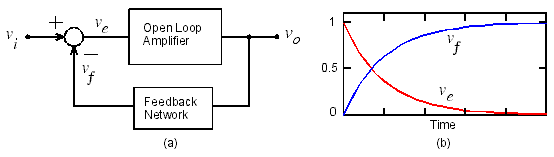
| Figure 1. (a) Amplifier block diagram. (b) Feedback and error voltage waveforms. |
A hot topic of amplifier design in the 1970s was "transient intermodulation distortion" (TIM). Other names which were used for this phenomenon were "slewing induced distortion" (SID), and "dynamic intermodulation distortion" (DIM). TIM occurs when a transient input signal overloads the input stage of an amplifier, causing it to either cut off or to become nonlinear for a brief instant before the feedback signal arrives. If the input stage cuts off, the amplifier output slews and the amplifier produces hard TIM. If the input stage becomes nonlinear but does not cut off, the amplifier is said to exhibit soft TIM.
To see how TIM can occur, consider the block diagram of a feedback amplifier given in Figure 1(a). The error voltage which drives the open-loop amplifier is the difference between the input voltage and the feedback voltage, i.e. ve = vi - vf. If the gain of the open-loop amplifier is very large, the steady state error voltage is very small and the input stage does not overload. Now, suppose a voltage step of 1 V is applied at the input, i.e. the input voltage is instantaneously increased from 0 to 1 V at time t = 0. The output voltage cannot change instantaneously so that vo = 0 at the time the input step occurs. At t = 0, there is no feedback, i.e. vf = 0, and the error voltage is ve = 1 V. As time increases, vo begins to increase, causing vf to increase which makes ve become small. This is illustrated by the waveforms in Figure 1(b).
|
| Figure 1. (a) Amplifier block diagram. (b) Feedback and error voltage waveforms. |
Suppose that the input stage to the amplifier modeled in Figure 1(a) is a conventional BJT diff amp. One BJT in a diff amp cuts off when the differential input voltage exceeds about 57 mV. The differential input voltage in Figure 1(a) is the error voltage ve, so that the diff amp would overload for ve = 0.057 V. It follows from Figure 1(b) that a 1 V step at the input would cause gross overload of the diff amp. There are two ways of increasing the overload voltage. One is to use resistors in series with the emitters of the BJTs. The other is to replace the BJTs with FETs. Because FET parameters are so unpredictable and FETs are more susceptible to flicker noise, I prefer the BJTs with emitter resistors. This is explained in more detail below.
The time delay before the feedback signal arrives at the input stage is set by the bandwidth of the open-loop amplifier. TIM cannot occur if the open-loop bandwidth is greater than the signal bandwidth. Thus a criterion that has been described for minimizing TIM is to design the open-loop amplifier to have a bandwidth greater than the audio band. To keep the amplifier stable, the product of the open-loop gain and the open-loop bandwidth must not be too large. Thus if the open-loop bandwidth is increased, the open-loop gain must simultaneously be decreased to keep the amplifier stable. With a low open-loop gain, such designs were said to be "low feedback amplifiers." I published an amplifier in Audio magazine which had an open-loop bandwidth of about 25 kHz and an open-loop gain of about 400. I called the article "Build a Low TIM Amplifier." With no feedback, the amplifier had a THD at 1 kHz of 0.5% at an output power of 50 W into 8 ohms.
Many of the critics of TIM disputed the design criteria that the open-loop bandwidth must be greater than the signal bandwidth to prevent TIM. After my article was published, I came to realize that this is true, provided the open-loop gain and bandwidth are varied in such a way that the product of the two remains constant. If this is done correctly, static distortions such as THD and IM can be reduced while not affecting the stability of the amplifier or its susceptibility to TIM. The product of the open-loop gain and bandwidth is called the gain bandwidth product. The original amplifier had a gain bandwidth product of 10 MHz. I have since decreased this to about 8 MHz because I feel that it improves stability and leads to a better sounding amplifier. The gain bandwidth product was decreased principally by increasing the value of the diff amp emitter resistors from 100 ohms to 300 ohms. This alone would have decreased the gain bandwidth product to below 8 MHz, but I simultaneously changed the transistors in the second stage to lower capacitance transistors which tended to increase it.
I could not even guess how many people built the original amplifier or the several versions that followed. I received mail from all around the world. It seemed to me that the interest in building it would never stop. By the early '90s, however, about the only people I heard from who wanted to build it were students. Then a former student sent me email and asked if I had my amplifier plans on the web. After I put a very brief set of plans on the web, I started getting email from people interested in the amplifier. The interest seemed to peak up when Georgia Tech hosted the "Olympic Village" during the 1996 Olympics in Atlanta. Every time I have received questions, I have tried to modify the plans to answer them. Thus the plans have gotten much more detailed than I had originally intended.
The Leach Amp, Vers. 4.5, is the latest update of the "Low TIM Amplifier." The Georgia Tech students who built it never referred to it as the "Low TIM Amplifier." They always called it "The Leach Amp." Over the years, I have seen countless versions of the amplifier built by students and others. All of the bugs have been worked out, and the amplifier should perform flawlessly if it is built with patience and care. This is an advanced construction project. I do not recommend that someone tackle it who has not had experience with electronic construction and assembly. If you don't know how to solder electronic components to a printed circuit board, this is not a project that I recommend. I recently had a student solder the components to his circuit boards and test them in one of our labs. He told me that they tested ok. I asked to see the boards. On one, the base lead to a transistor was not soldered. On the other, there was a cold solder joint through which the component lead could be pushed out of the hole in the board. If these had been left uncorrected, neither channel of his amp would have worked after connecting the output transistors to the circuit boards. You must know how to solder to tackle this project.
There was a mechanical engineering student at a school in New York state who tried to build an amplifier. I got several emails from him asking questions while he was building it. When he finished, he plugged the amp into the wall outlet, turned it on, and it flamed. I felt really sorry for the guy. His error was not double checking everything he did and he did not follow the test procedures that I described. One must check the circuit boards with a current-limited bench power supply before and after connecting the power transistors to them. Lacking a bench power supply, the amplifier power supply with a Variac transformer to vary the ac voltage can be used, but I don't recommend it. In this case, the circuit board fuses should be replaced with 100 ohm 1/4 watt resistors. If there is an error, these will smoke and protect the amplifier. This is all described in the Construction Details. I heard from one builder who said that his amplifier would have gone up in smoke if he hadn't followed my advice about the 100 ohm resistors. I never heard again from the student in New York after he said that his amplifier blew up.
When students ask me how long it takes to build the amplifier, I tell them to allot 3 months to order and acquire the parts and a second 3 months to build it. A former student thought he could build the amplifier in two weeks. Not only did he pay local vendors about twice what he could have ordered the parts for, but his amplifier was plagued with construction problems. In trying to solve the problems, he unsoldered and soldered parts to the circuit boards so many times that the traces started to peel up. He ended up having to get a new set of circuit boards and start over. After he graduated, he has ordered eight more boards to build more amplifiers.
With power supply voltages of about 58 V dc (+ and -), the amplifier will put out an average sine wave power of 120 watts per channel with an 8 ohm load. SMPTE IM distortion is typically 0.15% at clipping and less than 0.01% at lower levels. The circuit has a voltage gain bandwidth product of about 8.5 MHz and a large signal slew rate of 60 V per microsecond. Frequency compensation is provided by 300 ohm emitter degeneration resistors in the input differential amplifier stage, 10 pF lag compensation capacitors in the high gain stage, and feedforward compensation above 150 kHz around the driver and output stages. Voltage and current sensing protection circuits prevent damage to the amplifier in the event that the output is short circuited.
Some readers have questioned the 8.5 MHz gain bandwith product. This is not to be confused with the fT or gain bandwidth product of the output transistors. The fT of a transistor is the frequency at which its current gain is reduced to unity. In contrast, the gain bandwidth product of an amplifier is the product of the voltage gain and the frequency at which the gain is down by 3 dB or a factor of 0.707. Regardless of the amplifier circuit, this product cannot be made too large if the amplifier is to be stable and not oscillate. Setting the gain bandwidth product is part of what is called the "frequency compensation" of an amplifier.
The amplifier will drive a 4 ohm load to full power without current limiting. Depending on the power supply regulation, the output power with a 4 ohm load is as great as twice the power with an 8 ohm load. With loads lower than 2 ohms, the protection circuits limit the maximum output current, and thus the output power, to protect the output transistors. The amplifier is stable with capacitive loads and will drive electrostatic loudspeakers with no problems.
A good indicator of an amplifier sound quality is its ability to drive a capacitive load. The classic example of a capacitive loudspeaker transducer is the electrostatic transducer. Another is the piezoelectric transducer used in some horn tweeters. I have heard of amplifiers overheating when driving arrays of these tweeters. No doubt the circuits were oscillating. A third source of load capacitance that is often overlooked is the loudspeaker cable. Some of the so-called "high definition" cables are designed to minimize the series inductance. Because the series inductance per unit length multiplied by the shunt capacitance per unit length is a constant that is equal to the reciprocal of the velocity of light squared, minimizing the inductance maximizes the capacitance. Therefore, these cables can exhibit a high shunt capacitance. For this reason, I generally do not recommend them. I have heard of a certain "high-end" amplifier that is no longer made smoking when these cables are connected to its output, even with no signal input. A former student, who was working for Panasonic, performed a listening test in their "high-end" listening room to see if there was any audible difference between a "high definition" cable and ordinary zip cord. I do not know what power amplifier they used, but he said that the listeners were in agreement that the high-frequency response was better with the zip cord, no doubt because the high capacitance of the "high definition" cable.
The Low TIM amplifier is stable with capacitive loads. I have tested it with a 2 uF capacitor. This is a test that I learned from reading Bascom King's reports on amplifiers for Audio (rip) magazine back in the '70s, and it is probably the worst load that I know of. Because some amplifiers become unstable with a capacitor for a load, I have seen the test made with a resistor, e.g. a 2 ohm resistor, in series with the capacitor. This is cheating. It does not indicate the stability of the amplifier with a capacitive load. The first time I tested my prototype Low TIM amplifier with a 2 uF capacitor, it blew the 0.33 ohm 5 W emitter degeneration resistors in series with the output transistors. I suspect the circuit was oscillating. Either the resistors couldn't handle the current or the circuit was oscillating. I suspect the latter. These problems were solved before I finished the original prototype amplifeir.
Another good indicator of an amplifier sound quality is its high frequency clipping behavior. When an amplifier is driven into clipping, some of the transistors in the circuit are driven into saturation. When a transistor saturates, a relatively large charge is stored in the semiconductor junctions. For the amplifier to come out of clipping, this charge must be neutralized. To minimize the time for this to occur, the larger output and driver transistors should never be allowed to saturate. Although the power rating of an amplifier can usually be increased if the output transistors are allowed to saturate, it causes a high frequency clipping problem that has been described as "sticking." When an amplifier exhibits this problem, its output waveform appears to become "stuck" at the clipping level when it is driven into clipping at high frequencies. In the Low TIM amplifier, the transistors which saturate are in the second stage of the amplifier. As a result, sticking problems are minimized when the amplifier is driven into clipping.
The data displayed in Figures 2 through 5 were measured on student Allen Robinson's amplifier with an Audio Precision System II analyzer. Figure 2 shows the plot of the measured gain versus frequency over the band from 20 Hz to 20 kHz. Below 10 kHz, the gain is 26.6 dB, decreasing to 26.5 dB at 20 kHz. The gain was measured with an input voltage of 1 V rms with an 8 ohm load. At this level, the output power is 57 W.
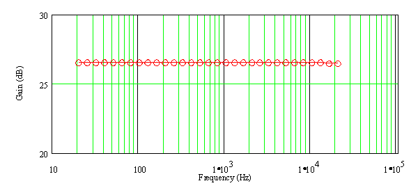 |
| Figure 2. Measured gain in dB versus frequency. |
Figure 3 shows the plot of the measured phase versus frequency over the band from 20 Hz to 20 kHz. As with the gain measurement, the phase was measured with a 1 V rms input signal and an 8 ohm load. At 20 Hz, the phase is +1.5 degrees, decreasing to -8.8 degrees at 20 kHz. If a linear scale were used for the frequency axis, the phase plot would be a line with a constant slope. The slope corresponds to the time delay through the amplifier which is approximately 1.5 microseconds.
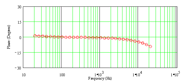 |
| Figure 3. Measured phase in degrees versus frequency. |
Figure 4 shows the measured total harmonic distortion versus frequency at an output power of 120 watts into 8 ohms. At 20 Hz, the distortion is 0.006%. It increases to 0.29 % at 20 kHz. The rise in distortion at higher frequencies is a characteristic of a low feedback amplifier. It is caused by the decrease in loop gain above the first pole frequency in the amplifier transfer function. The loop gain decreases at 20 dB per decade above the first pole, causing the distortion curve to increase at high frequencies. The feedforward compensation around the output stage at high frequencies also contributes a little to the rise. At lower power levels, the distortion is less, especially at the higher frequencies.
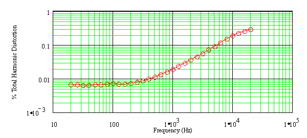 |
| Figure 4. Measured THD plus noise versus frequency at 120 W output. |
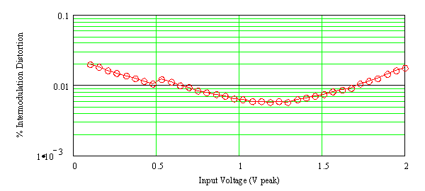
Figure 5 shows the measured intermodulation distortion versus input level with an 8 ohm load. The distortion was measured using the Society of Motion Picture and Television Engineers (SMPTE) standard. The input signal is the sum of a 60 Hz sine wave and a 4 kHz sine wave having an amplitude ratio of 4 to 1. The analyzer measures the percent modulation distortion on the smaller amplitude 4 kHz wave caused by the larger amplitude 60 Hz wave. The input voltage was swept from 0.1 V peak to 2 V peak for the measurements. The amplifier is at the threshold of clipping when the input voltage is 2 V peak. At this level, the IMD is 0.018%. At lower levels, it decreases to 0.0059% and then increases as the level is decreased further. The rise in IMD at the lower levels is caused by residual noise and hum in the measurement system. Although the hum and noise is constant, it increases when expressed as a percent of the output voltage when the input voltage is decreased.
Since making these measurements, I have discovered that the Audio Precision analyzer puts out a constant low-level noise that gets amplified by the amplifier and causes the distortion to measure higher than it should at low power levels. No doubt, this is the reason for the rise in IM distortion at low levels in Figure 5. A student discovered this in testing his amplifier. The solution he found was to increase the output level of the analyzer and use an attenuator between it and the amplifier. I need to retest Allen's amplifier with the attenuator. The distortion at low levels should be lower that what is shown in the graph.
 |
| Figure 5. Measured IMD versus input voltage. |
This page is not a publication of the Georgia Institute of Technology and the Georgia Institute of Technology has not edited or examined the content. The author of this page is solely responsible for the content. Copyright 2004. All rights reserved.