 |
| Figure 1. Amplifier input stage. |
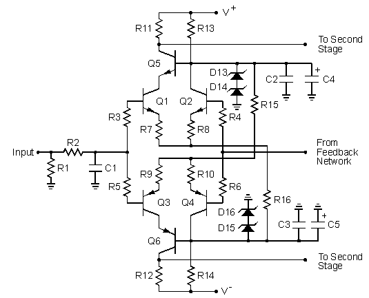
The input stage to the amplifier is shown in Figure 1. R1 sets the input resistance at 20 kohm. R2 and C1 form a 200 kHz input low-pass filter to protect the amplifier from unwanted RF signals at the input. Q1 through Q4 form a complementary diff amp input stage. The input signal is applied to the bases of Q1 and Q3 while the feedback signal is applied to the bases of Q2 and Q4. The diff amps subtract the feedback signal from the input signal to generate error signals which drive the following stages in the amplifier. The error signals are the collector currents in Q1 and Q3. In addition to being part of the input low-pass filter, C1 improves the bandwidth of the feedback signal path through the diff amps for improved phase margin in the loop-gain transfer function.
|
| Figure 1. Amplifier input stage. |
Q5 and Q6 form cascode common-base stages which conduct the diff amp error currents to the load resistors R11 and R12. Q5 and Q6 also function to reduce the voltage across Q1 - Q4 by about 18 V to prevent voltage breakdown in these transistors. Diodes D13 through D16 are 20 V Zener diodes which regulate the voltages that set the bias currents in the diff amps. Each zener diode is biased at a current of about 3.3 mA. Although a single zener diode could be used in place of two series diodes, I have found that the error tolerance in the voltage is less with the series connection of 2 diodes. C2 through C5 are ac decoupling capacitors which ensure the bases of Q5 and Q6 are at ac signal ground. R15 and R16 set the tail bias current in each diff amp to about 3.25 mA. This current and resistors R7 through R10 set the differential tansconductance gain of the diff amps at about 1.6 mA/V. The diff amps use resistive tail current bias circuits. Not only do these generate less noise than active current sources, but they provide a smooth amplifier turn-on that is free of thumps. The voltage gain of each diff amp is approximately 2, i.e. 6 dB.
R7 through R10 are emitter degeneration resistors which play an important part in the frequency compensation of the amplifier. Without these resistors, the gain of the diff amps would increase to about 40, i.e. to 32 dB. If the theory can be believed, the distortion would simultaneously decrease by a factor of 40. However, this would seriously degrade the stability of the amplifier from oscillations unless the diff-amp bias currents are decreased, the compensation capacitors in the second stage are increased, or both so as to maintain the same gain-bandwidth product. Either would degrade the slew rate.
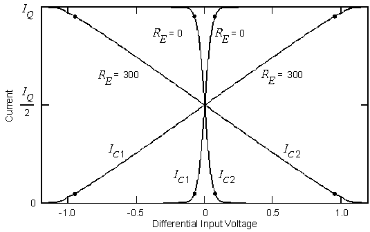
R7 through R10 not only decrease the gain of the diff amps, but they also improve its linearity and dynamic range. This is illustrated in Figure 2 which shows plots of the collector currents in Q1 and Q2 (or Q3 and Q4) as a function of the differential input voltage with and without the emitter resistors. The current IQ is the diff-amp bias current which is about 3.25 mA. The linear range is taken to be the region between the dots where the currents vary between 5% and 95% of the maximum value. Without the resistors, the diff amps leave the linear range when the differential input voltage exceeds about 57 mV. With the emitter resistors, this voltage is increased to about 951 mV, or by a factor of about 17 (24 dB). This reduces the susceptibility of the amplifier to the transient types of distortion known as slewing induced distortion (SID), transient intermodulation distortion (TIM), and dynamic intermodulation distortion (DIM). The figure shows that with the emitter resistors, the diff amp is linear with input voltages as large as 1 V.
 |
| Figure 2. Plots of the diff amp currents versus differential input voltage. |
Most of the amplifier circuits that I have seen either do not have emitter degeneration resistors in the input diff amps or the value of the resistors is small compared to the 300 ohm values in the Low TIM amplifier. I have even seen some circuits in which the resistors are present but capacitors are used to bypass them for AC signals. These amplifiers usually have a very high open-loop gain, i.e. the gain before feedback. This makes the distortion lower when feedback is added, but they tend to oscillate unless large value compensation capacitors are used. This reduces the amplifier slew rate and increases the susceptibility to transient distortion problems.
The Low TIM amplifier is designed for a specified gain-bandwidth product and slew rate. I chose a gain-bandwidth product of about 8.5 MHz. This is low enough to qualify the amplifier as a low-feedback design. However, it is high enough to give both low distortion figures and a closed-loop bandwidth that is over 400 kHz before the addition of the input low-pass filter (R2 and C1). I chose a slew rate of about 60 volts per microsecond. This is much higher than required. It is high enough to give a large-signal bandwidth of around 220 kHz. However, I never recommend anyone to test the amplifier at full power above 20 kHz. The output transistors are put under severe thermal stress during such tests, and they can fail. I know someone who used a Low TIM amplifier to drive an ultrasonic shaker table at full power at a frequency of 40 kHz. He said it worked, but I don't recommend such applications.
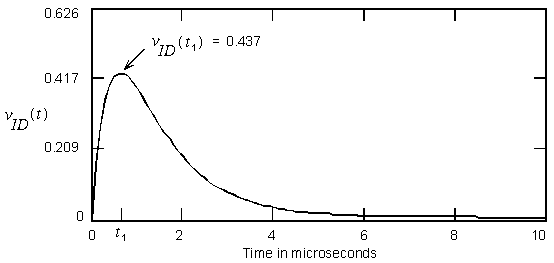
The bandwidth of the input low-pass filter (R2 and C1) is chosen so that it is impossible for the amplifier to slew before it clips. Figure 3 shows a plot of the differential input voltage vID to the diff amps for a step input voltage which drives the amplifier to the verge of clipping. The peak value occurs at time t1 which is about 0.6 microseconds. The peak value is 0.437 V. For a square wave input signal, this peak is increased by a factor of 2 to 0.874 V, which is within the range of linear response of the diff amp illustrated in Figure 2. Thus the amplifier cannot slew before it clips with a square-wave input signal. This is the worst case test for slewing.
 |
| Figure 3. Plot of the differential input voltage for a voltage step input. |
This page is not a publication of the Georgia Institute of Technology and the Georgia Institute of Technology has not edited or examined the content. The author of this page is solely responsible for the content.