Transistor Matching
For minimum dc offset at the output, Q1 through Q4 should preferably have matched current gains. The current gains can be measured with a curve tracer or with a multimeter which has this capability. Ideally, all four transistors should be matched. If this cannot be achieved, the second choice is for Q1 and Q3 to be matched and Q2 and Q4 to to be matched. The third choice is for Q1 and Q2 to be matched and Q3 and Q4 to be matched. The typical dc offset at the amplifier output is less than 50 mV. If you are concerned about how well the transistors are matched, I have seen amplifiers built without matching the input transistors, and they had no dc offset problems.
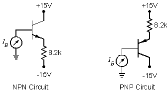
If you do not have access to a curve tracer, the circuits in Figure 1 can be used to match the transistors. These circuits can be easily assembled on a solderless electronic breadboard. The bias current in each transistor is set at approximately 1.6 mA. Matched transistors will have equal base currents. The expected current should be in the approximate range from 4 uA to 20 uA.
 |
| Figure 1. Transistor matching circuits. |
When using these circuits to match transistors, the power supply voltages should be held constant. Don't turn the voltage down or off when changing transistors. If the measured current appears to be unstable, the transistor may be oscillating or picking up a RF signal. In this case, a 0.1 ufd capacitor from base to emitter should cure the problem. You may notice some temperature drift of the current as the transistors warm up. You can use 9 V batteries in place of the 15 V sources if you change the 8.2 kohm resistors to 4.7 kohm.
If you do not have a multimeter that reads microamps, you can put a 51 kohm resistor in series with the base and measure the voltage across the resistor. Matched transistors will have equal voltages. The expected voltages should be in the approximate range of 0.2 V to 1 V.
Zener Diode Matching
The bias currents in the diff amps are regulated by zener diodes. In each diff amp, two 20 V diodes are used in series to form an equivalent 40 V zener. Although a single diode could be used, the error tolerance is less when two diodes are used in series. If you are building a stereo amp, you need 8 diodes. It is probably cheaper to buy a single pack of 10. I prefer to measure the zener voltage of each and pick series combinations of diodes that give equal reference voltages on each circuit board. It is not necessary to have exactly +40 V and -40 V. But the two voltages on each circuit board should be as close as possible to minimize dc offset problems.
The zener voltage of a diode can easily be measured by connecting a resistor in series with it on an electronic breadboard and connecting a bench power supply across the series combination. The power supply voltage should be set so that the current through the diode is 3.3 mA. If you don't have a current meter, the voltage across the resistor should measure 3.3 x R, where R is in kohms. For example, the voltage across a 2 kohm should be 6.6 V. Once the current is set, the dc voltage across the zener diode can be measured with a voltmeter. For example, if you have +15 V and -15 V supplies, connect the diode in series with a 3 kohm resistor across the two outputs and measure the diode voltage. If you get the diode backward, the resistor will get hot.
Assembly of Circuit Boards
Click here to see the layout of parts on the component side of the circuit board with the copper traces beneath the board shown. Click here to see the layout without the copper traces. Start assembly of the circuit boards by soldering the smallest components first, working up to the largest components last.
If you do not know how to solder, please find someone who can teach you. Do not use a soldering iron that gets too hot. I like the temperature regulated Weller irons, but they get a little pricey. If you use a non-temperature regulated iron, it should have a power rating of about 30 watts maximum. The principle reason for poor solder joints is not enough heat. But too much heat can damage a component or make a pad on the circuit board peel up.
To get a good solder joint, simultaneously apply the tip of the iron and the solder to the circuit board so that they touch each other and touch both the wire being soldered and the solder pad, i.e. all 4 are in contact. When the solder begins to flow, remove the solder and hold the iron on the joint until the solder flows and bonds to the wire and the pad. Then pull the tip of the iron up so that it slides up the wire. A good solder joint is smooth and shiny. It doesn't have any waves in it and it doesn't look like a drop of water on a waxed car. Figure 2 illustrates what a correct solder joint looks like. It also shows one where too much solder is used and one where not enough heat is used. In the latter case, the solder is bonded to the pad on the circuit board but not to the wire. When you cut the wire, cut it just above the solder joint. Do not cut into the solder.
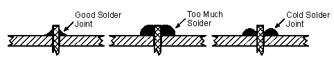 |
| Figure 2. Good and bad solder joints. |
The assembly procedure is approximately as follows:
- Install and solder the short-circuit jumper labeled J on the circuit board layout near Q17. If you use a single nonpolar capacitor for C6 (as opposed to the two polar capacitors C6A and C6B as described in the Parts List), solder a short-circuit jumper in the holes for C6B.
- Install and solder the resistors. A resistor lead bender should be used to bend the leads for the proper length. No more than about 5 resistors should be soldered and clipped at a time. Check the value of all resistors with an ohmmeter before soldering them to the circuit board. I saw one amp which had 33 kohm resistors where I specified 3.3 ohms. Another amp had a 12 kohm resistor where there should have been a 1.2 kohm resistor. This caused a bad dc offset problem.
- If there is a problem with the VBE multiplier bias circuit, it could cause R36 to smoke and even catch on fire. To minimize damage to the circuit board in this event, I recommend stripping two 1/4 inch pieces of insulation from some hookup wire and putting them on the leads of R36. This will cause R36 to stand up off the circuit board to minimize damage in the event that it smokes. If it does smoke, you can lose expensive output and/or driver transistors, so be careful and don't make errors.
- Install and solder Q1 through Q11. Don't bend their leads before putting them on the board. Their cases should be about 3/16 inch off the board. Figure 3 shows the pinouts of all of the transistors.
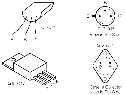 |
| Figure 3. Transistor pinouts. |
- Install and solder Q12 through Q15. These transistors should be flush with the board.
- Install and solder Q16 and Q17. First, use needle nose pliars to bend the transistor leads at 90 degrees so that they will mount on the circuit board with the hole in the metal tab on the transistor mating with the hole in the circuit board. Then put the transistor and its TO-220 heat sink on the circuit board and secure them with #4 machine screws and nuts. Solder and clip the transistor leads. It is not necessary to use any insulating wafer between the transistors and heat sinks. If you use the clip-on version of the TO-220 heat sinks, don't trust the clips without the screws to make good thermal contact between the transistors and the heat sinks. Screw them down to the circuit board.
- Install and solder L1/R49. This is a 2 W resistor with an inductor wound around it. Figure 4 illustrates this part. There are 11 to 12 turns of wire around R49. Instructions for winding the inductor are given in the Parts List.
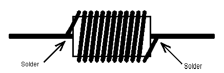 |
| Figure 4. L1 wound around R49. |
- When all components are soldered to the circuit board, the flux should be removed with a solvent such as Stripper brand circuit board spray cleaner and a soft bristle brush. If this is not done, noise problems can arise that are caused by random pulses of current through the flux. I once saw flux catch on fire when it bridged the trace of a power supply rail and a ground trace.
Testing the Circuit Boards
The circuit boards should be tested with a bench power supply before they are installed in the chassis. Because there will be no bias current in the driver stage, a small amount of crossover distortion might be observed on the output voltage waveform during these tests. This distortion appears as a "glitch" on the oscilloscope waveform when the output voltage crosses the zero voltage level. At the higher frequencies, the "glitch" moves off the zero crossing level and tends to "climb up" the waveform. The initial test procedure is as follows:
- Temporarily tack solder two 100 ohm resistors to the back of each circuit board, one from the loudspeaker output to one side of R36 and the other from the loudspeaker output to the other side of R36.
- Tack solder a short circuit jumper in parallel with C12.
- Connect the positive, negative, and common outputs from a dual power supply to the board. Note that there are two circuit board grounds to which the power supply common must be connected, one is near the input and the other is near the output. The power supply output voltages should be set to zero and the current limits should be set to about 50 mA. If the power supply does not have a current limit function, connect a 100 ohm 1/4 watt resistor in series with the positive and negative power supply leads.
- With a signal of about 1 V peak at 1000 Hz connected to the input and a dc coupled oscilloscope connected to the output, slowly turn up the power supply voltages. The circuit should amplify without drawing more current than about 25 mA when the power supply voltages are about 8 V dc or greater, not to exceed 60 V dc. The output signal will initially be a clipped sine wave until the power supply voltages are increased.
Several additional tests should be performed on each circuit board before it is disconnected from the power supply. These are as follows:
- At 1000 Hz, the gain should be approximately 21 (26.4 dB) and should remain constant in the 20 Hz to 20 kHz band.
- The lower -3 dB cutoff frequency should be approximately 1 Hz. The upper -3 dB cutoff frequency should be approximately 140 kHz. At the -3 dB cutoff frequencies, the gain should be approximately 14.8 (23.4 dB).
- The clipping response should be symmetrical and clean with no evidence of "sticking". That is, the clipped voltage peaks should not appear to "stick" at the clipping voltage.
- At 20 Hz, the square wave response should exhibit a slight amount of tilt.
- At 20 kHz, the square wave should be slightly rounded.
- Absolutely no ringing should be observed on the output square wave at any frequency.
- With the input signal generator disconnected, the dc voltage at the output should not exceed 100 mV, preferably less than 50 mV. Mismatched + and - power supply voltages can affect this.
Drilling the Heat Sinks
The heat sinks should be marked, drilled, and deburred carefully. You can lose expensive transistors if a short circuit occurs in a heat sink or if a burr penetrates an insulating wafer between a power transistor and a heat sink. The heat sink for each channel is drilled so that the four output transistors mount in the channel with the four temperature sensing diodes in the center. This is illustrated in Figure 5. A procedure for drilling the heat sinks is as follows:
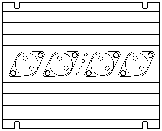 |
| Figure 5. Heat sink view. |
- Click here to see an Adobe Acrobat file that contains a template for drilling the heat sinks. Use the template and a center punch to tap the hole positions for the power transistors and bias diodes. There is a line on the printout that should measure exactly one inch. If it does not measure one inch, you must change the Acrobat print settings so that it prints to the correct dimensions.Every time a new version of Acrobat comes out, it seems that the print image size changes and you have to fiddle with the print settings. Do not use the template if you cannot get it to print to the correct dimensions.
- Use a drill press, not a hand drill, to drill the holes. To prevent burrs, use sharp drill bits and drill into the side of the heat sink wall on which the transistors mount. Drill pilot holes first with smaller size bits. The hole diameter for the transistor mounting hardware is normally 1/4 inch. The hole diameter for the bias diodes must be determined with a drill index.
- Any burrs around the holes should be removed by spinning a larger size drill bit in the holes with the fingers. Do not use pressure when doing this, or excessive metal can be removed. Double check for burrs by rubbing your fingers along the heat sink surface. All burrs must be removed or they can puncture an insulating wafer and cause a short circuit.
Installing the Bias Diodes
You should be careful when you assemble and install the bias diodes. If a diode is forced into a hole in the heat sink that is too small, its case can crack. I once saw a student's amplifier that randomly blew power supply fuses. We traced the problem to a cracked diode. He was lucky that the power transistors didn't blow. Figure 6 illustrates the installation of the diodes in the heat sink walls. There are 6 bent leads which must be insulated with insulation removed from hookup wire before being bent. There are 5 joints which must be tie wrapped, soldered, and insulated with heat shrink tubing. The diodes are glued into the heat sink with instant bonding glue. Do not use the gel version of this glue. It does not flow and will end up on the outside of the heat sink.
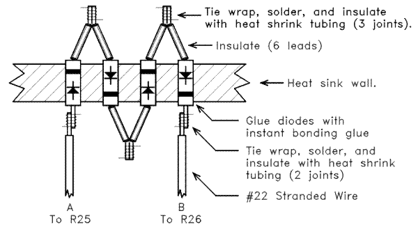 |
| Figure 6. View of diodes in heat sink wall. |
Use the following procedure to install the diodes:
- The first step is to prepare the two wires which connect diodes D1 and D4 to the circuit boards. The current which flows in these wires is very small. For this reason, you do not need to use a large size wire. I recommend #22 stranded (never use solid) wire. Strip about 3/16 inch of insulation from one end of each wire.
- The next step is to tie wrap the wires to D1 and D4. Use a single strand from a piece of #22 stranded hookup wire to tie one wire to each diode. I find this easier to do before I cut the diode leads. One wire connects to the unbanded end of D1 and the other connects to the banded end of D4. Hold the diode lead, the #22 wire, and the single strand between the fingers of one hand. Grasp the single strand with the fingers of the other hand and spiral wrap four or five turns around the diode lead and the #22 wire.
- Solder the wrapped joint. I like to clamp the diode in a small vice when doing this. Then cut off the excess diode lead and the two ends of the single strand of wire. Insulate the joint with heat shrink tubing.
- Install the four diodes in each heat sink using instant bonding glue to secure them. Do not force a diode into its heat sink hole. Any raised spot on the body of a diode can be filed off to make the diode fit.
- After the glue sets up, put a 3/8 inch length of insulation stripped from a piece of hookup wire over the 6 exposed diode leads. Push the insulation down until it is flush with the diode body so that a diode lead cannot make contact to the heat sink..
- Bend the 6 insulated diode leads as shown in Figure 6 so that they are at an angle of approximately 45 degrees with the heat sink wall. Bend the ends of the leads so that they are parallel as shown in the figure. Tie wrap the parallel leads together with a spiral wrapped single strand from #22 stranded hookup wire. Two needle nose pliars make this tedious operation simpler. Solder the wrapped wires.
- Cut off the excess diode lead lengths and insulate the solder joints with heat shrink tubing.
- The #22 stranded wires connected to D1 and D4 should be loosely twisted together before soldering to the circuit board.
- Double check the diode assembly. If a diode is backward, the output transistors can blow. You can check the diode polarities one at a time with an ohmmeter. The ohmmeter will not have enough test voltage to forward bias all 4 diodes simultaneously. If there is a short circuit between a diode lead and the heat sink metal, the amplifier will not work and the output transistors can be blown.
Installing the Power Transistors
The procedures for installing the 4 power transistors on each heat sink are as follows:
- The wires which connect the sockets for Q18 through Q21 to the circuit boards should be soldered to the sockets before they are installed in the heat sinks. I recommend #18 or #20 stranded wire. A small vice can be used to hold the sockets when soldering the wires.
- The next step is to install the insulating wafers on the power transistors. I prefer the flexible rubber insulators (Digi-Key BER100, Bergquist number SP600-05) because they do not require any heat sink compound. If mica wafers are used (DigiKey 4662K), coat both sides with a thin coating of heat sink compound. This is messy stuff to work with. If you use too much, it will squeeze out when the transistor mounting screws are tightened to make a bigger mess.
- Put an insulator on each power transistor, put the transistor on the heat sink, and install the socket. Use the proper screws to secure the sockets to the transistors. Some sockets use machine screws while others use sheet metal screws. A nut on the screw is never required if the proper type screw is used. I once had a student who used the sockets which require sheet metal screws. Too lazy to go out and buy sheet metal screws, he used machine screws and nuts to secure the sockets. When he finished the amplifier, we found that he had the NPN and PNP power transistors interchanged. We couldn't remove the transistors without first removing the heat sinks from the chassis to get to the the nuts on the machine screws. However, the wires between the circuit boards and the power transistor sockets were too short to remove the heat sinks. The student had a mess which could have been avoided if he had used the correct screws on the transistor sockets.
- Use an ohmmeter to check for short circuits from each transistor lead to a bare metal spot (not the black anodize finish) on the heat sinks.
Preparing the Rear Panel
The following instructions apply to both the Moduline chassis and the Mark 5 chassis. A view of the parts layout on the inside of the rear panel is shown in Figure 7. Not all of the wiring is shown in this figure. The heat sinks mount on the other side of the panel. The circuit boards should be mounted so that the component side is away from the panel. Otherwise, you cannot get to the bias pot to set the bias current.
 |
| Figure 7. Layout of the rear panel. Keep the input leads away from all other circuit board leads. |
- It is easier than you think to scratch the chassis. I recommend putting masking tape on it before drilling it. When you go to remove the tape, heat it with a hair dryer to make it easier to pull off. Otherwise, you might pull some paint off. When working with the chassis, always place a thick towel on the workbench to prevent scratching it.
- The heat sinks are mounted on the outside wall of the rear panel. I recommend mounting the heat sinks vertically so that warm air can rise through them. However, the heat sinks will protrude at the top of the amplifier. If you don't like this, you can mount the heat sinks horizontally. Many students who have built the amplifier have done this, and I have heard of no thermal problems. The top panel of the chassis will not fit if the heat sinks are mounted flush with the back panel. I recommend mounting each heat sink with four 1/2 inch #4 machine screws (DigiKey H146) with 1/4 inch unthreaded standoffs (spacers) (DigiKey J167) around the mounting screws between the heat sinks and the rear panel. An option is to use nuts as shims in place of the stadoffs. Mating holes must be drilled through the heat sink flanges and through the back panel for the screws.
- The circuit boards are mounted on the inside wall of the back panel. The input sides of the boards should be at the center of the panel. The circuit boards should be mounted on standoffs (spacers). I recommend 3/4 inch #4 threaded standoffs (DigiKey J240) with 1/4 inch #4 machine screws (DigiKey H142) to mount the boards. If you use shorter standoffs, you will have problems fitting the wires between the circuit boards and the rear panel.
- Mark and use a center punch to tap the positions of the holes in the back panel for the AC line cord, the phono input jacks, the loudspeaker output jacks, the heat sink and circuit board mounting screws, and the wires which connect the circuit boards to the heat sinks. The standard spacing between the two 5-way binding post output jacks is 3/4 inch. I prefer putting the hole for the line cord under the loudspeaker output jacks for one channel. A strain relief or a grommet should be used around the line cord and the hole should be drilled to fit this. When you drill the holes, use a drill press, not a hand drill. I recommend first drilling pilot holes with a small size drill bit.
- There are 14 wires which connect between each circuit board and its heat sink. The holes for these wires must be large enough for all the wires to fit. You can use two smaller holes for the 14 wires in place of one large hole.
- Insulating rubber grommets must be used in the holes for the AC line cord and the heat sink wires. These grommets must be put in the holes before the wires are.
- The two input jacks should be in the center of the back panel between the heat sinks. The output jacks should be on the outsides. The AC line cord can be near the lower edge of the rear panel under the input jacks or on either side beneath an output jack.
- The input and output jacks do not make electrical contact to the rear panel.
Assembling the Rear Panel
The procedure for assembling the rear panel is as follows:
- Install the input jacks. Insulating washers must be used around each jack to insulate the ground side from the panel. Some of these washers are designed so that you use 2 shoulder washers on each jack. Others are designed so that you use one shoulder washer and one flat washer. If you use a second shoulder washer in place of the flat washer for the second type, it may be impossible to tighten the nut on the jack so that it cannot rotate in the panel.
- Install the output jacks. If you use the dual 5-way binding posts, tighten them carefully. I have cracked these when I tightened them to much.
- Mount the heat sinks with the power transistors and connecting wires to the outside wall of the panel with the wires inserted through the grommet insulated holes.
- Place the panel on a towel covered work surface with the heat sinks facing away from you. Lay the circuit boards close to and in front of the panel with the component sides down. The loudspeaker output sides of the circuit boards should be toward the outside of the rear panel. In case you ever have to repair the amplifier, you want the wires which connect the circuit boards to the heat sinks to be just long enough so that the boards can be folded down in this position without unsoldering any wires.
- Cut and strip the wires from the heat sinks so that they are just long enough to reach the boards with no tension after they are soldered. Don't make the wires any longer than necessary. I case of problems, you must be able to fold the board down for access to its rear. For this reason, all of the wires should route around the bottom edge of the board. Solder the wires to the circuit boards.
- Solder the power supply and central ground wires to the boards. Remember that there are two wires per board that connect to central ground. The ends of these wires which are not soldered to the boards are not connected yet.
- Solder wires between the circuit board outputs and the output jacks. These wires should be just long enough so that the boards can be folded down from the rear panel without unsoldering them. Note, the ground connections on the output jacks connect to central ground, not to the circuit boards.
- Solder input cables between the circuit board inputs and the input jacks. These cables should also be long enough so that the boards can be folded down from the rear panel without unsoldering them. A shielded cable or a twisted pair of #22 stranded wire can be used for the input cables.
- After all wires are connected to the circuit boards, the boards can be installed on the standoffs on the rear panel. Be careful not to pinch the wires between the circuit boards and the rear panel.
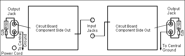
- Solder R50, C25, and the central ground wires to the ground terminals on the output jacks. Note, the output grounds do not connect to the circuit boards, they connect to central ground.
This completes the rear panel assembly. I recommend that you test the two channels with a bench power supply before proceeding. Adjust P1 for maximum resistance. If you use the potentiometer that I specified, the shaft should be fully counterclockwise for maximum resistance. Then perform the same tests made previously on the circuit boards. If too much current is drawn, D1 through D4 are probably wired wrong or P1 is not adjusted for maximum resistance.
Wiring the Chassis
Important points to remember: (a) Keep the wires from the power transistors to the circuit boards as short as possible, but long enough so that the circuit boards can be folded down in case a component has to be unsoldered. (b) Keep the leads to the input jacks away from all other wiring to the circuit boards. Otherwise, the output signal can capacitavely couple back into the input leads and cause damaging oscillations. (c) Keep the leads to the input jacks away from the power cord. Otherwise, a hum signal can be induced in the input. (d) If you use a shielded twisted cable for the input leads, ground the shield at only one end. (e) The routing of the 2 ground wires that go from the circuit board to the central ground seems to play a role in hum pickup. You may have to experimentally route these wires to minimize the hum.
The chassis should be wired before the rear panel is installed. A suggested layout for the chassis is shown in Figure 8.
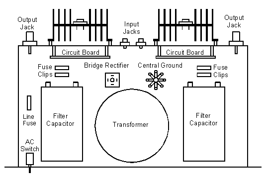 |
| Figure 8. Top view of chassis layout. |
Some of the considerations in wiring the chassis are as follows:
- The transformer should be mounted close to the front panel to prevent hum pickup. This also provides better balance if you pick up the amplifier from the front. The transformer may be heavy enough to cause the bottom panel to sag. To provide support, a strip of aluminum the width of the box that is bent in the shape of a shallow U can be installed under the transformer. The filter caps, bridge rectifier, and central ground terminal can also be installed on this strip. An alternate solution is to mount a rubber "foot" under the transformer to prevent the bottom panel of the box from sagging.
- If the filter caps are too tall to mount vertically, they can be mounted horizontally. Standard capacitor mounting hardware should be used.
- The central ground point can be made with a #4 or #6 machine screw through the bottom panel with several #4 or #6 solder lugs and a nut over it inside the box. The solder lugs must make good electrical contact to the bottom panel. Do not use Radio Shack solder lugs.
- The following wires connect to the central ground point: the green wire on the AC line cord, the ground wires for the filter caps, the transformer center tap, two ground wires from each circuit board, and the two loudspeaker ground wires.
- A solder lug terminal strip can be used for binding posts in the chassis wiring where needed. I recommend using one of these to connect the AC line cord to and for the power supply wiring.
Optional Input Level Control
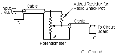
Several people have asked about a level control for the amplifier. I recommend a 10 kohm to 25 kohm log (or audio) taper potentiometer for the control, although a linear pot can be used. You can use either two single pots or a dual pot. An excellent pot is the Radio Shack 271-1732C 100 kohm dual pot. This is made by Alps, and you will see their name on the side of it. (I don't recommend any of their other pots.) I like to add two 16 kohm resistors to it to make it look like a lower resistance pot. Solder a resistor from the wiper to the input terminal on each side of the pot. Figure 9 shows how the pot is wired. When the pot shaft is rotated counter clockwise, you should measure a short circuit between the wiper and the ground terminal. The ground in the figure it marked G. Note that it connects from the input jack through the shield of the first cable to the pot and through the shield of the second cable to the circuit board.
 |
| Figure 9. Wiring for level control. |
Initial Tests on the Completed Amplifier
When the amplifier is completed, the following tests should be made:
- Test the power supply before installing fuses F2 - F5. The dc voltages should correspond to the values given in the power supply parts list for the transformer used. If the power supply is wired wrong, fuse F1 will blow. If a variac (variable autotransformer) is available, use it between the amplifier and the AC line to slowly increase the ac voltage from 0 V to 120 V AC for this test.
- The filter caps must be discharged before installing F2 - F5. Do not short circuit the capacitors to discharge them! You will get a loud pop and a big spark. A 100 ohm 2 W resistor is recommended to discharge the capacitors, but it can get hot! Use pliers to hold the resistor across the terminals of each capacitor for at least 30 seconds to discharge the caps.
- Adjust P1 on each circuit board for maximum resistance and install the power supply fuses. If the previous tests have been successful, you can proceed to the next step where you power up the amplifier. Again, I recommend the use of a variac to slowly increase the AC input voltage from 0 V to 120 V for this test. If you are unsure of anything, remove F2 - F5. Substitute a 100 ohm 1/4 W resistor for each of these fuses. You may wish to power up only one channel at a time.
- With no load connected to the amp, it can be powered up. If anything is wrong, the 100 ohm resistors in place of the power supply fuses will limit the current. They will
also smoke! The dc voltage drop across the 100 ohm resistors should be less than about 2.5 V (25 mA or less) if nothing is wrong. If this test is successful, turn the amp off and wait for the power supply to discharge. Remove the 100 ohm resistors and install F2 through F5.
Setting the Bias Current
If the preceding tests are successful, the next step is to set the bias currents in the output stages. This is done as follows:
- The power should be turned off and the power supply discharged.
- Remove F2 and clip an ammeter across the fuse terminals.
- Power the amp up with no input signal or load. Adjust P1 for the channel connected to F2 for a current of 100 mA. Be careful. Once I accidentally blew the output transistors in one channel of an amplifier I was building when I mistakenly tried to adjust P1 for the wrong channel.
- As the amp warms up, the current will drift. Readjust P1 until the drift stops. This will take about 10 minutes.
- Turn the amp off. Wait until the power supply discharges, then install F2.
- Remove F3 and repeat this procedure for the other channel.
- When the bias is adjusted properly, a dc voltmeter will read close to 3.4 V across Q7, i.e. across the collectors of Q12 and Q13. The collector of these transistors is the round metal case.
Is there a hum in the loudspeaker?
If a hum is encountered with the amp, install a 2-prong to 3-prong adapter on the AC input plug. This will eliminate any hum caused by a ground loop in the external AC wiring. However, the amplifier chassis will no longer be connected to safety ground. If the adaptor fails to get rid of the hum, it might be caused by a ground loop inside the amplifier. The following procedure can be used to determine if this is the case:
- Turn the amplifier off and wait for the power supply to discharge.
- Disconnect one input cable.
- Turn the amplifier back on.
- If the hum is gone, it is due to an internal ground loop. If the hum remains in the channel that has its input connected, the hum is probably in the source.
If you are sure that the hum is due to an internal ground loop, the procedure for breaking this loop is as follows:
- Turn the amplifier off and wait for the power supply to discharge. Do not perform this procedure with the amplifier on.
- Cut the wire to the central ground on the input side of one circuit board.
- Solder a short circuit jumper wire between the ground lugs on the two input jacks.
- The circuit board with the cut ground wire is now grounded back through its input ground lead to the ground of the other circuit board. Use an ohmmeter to verify the new ground connection before turning the amp back on.
Hints if Problems are Encountered
If problems are encountered, a list of things to check is as follows:
- Double check all wiring.
- Check to see that the bias diodes D1 - D4 are installed correctly, that none are cracked, and that the attaching leads make proper contact.
- Check the orientation of each diode and the polarity of each electrolytic capacitor.
- Check the orientations of Q1 through Q11.
- Are all transistor part numbers correct?
- Are any NPN and PNP transistors interchanged? I have embarrassed many students when I found this error in their amplifiers.
- Do the leads to the heat sinks connect to the right points on the circuit boards? I recently saw a student's amplifier where the base leads for the npn and pnp output transistors on one channel were reversed on the circuit board. The bias potentiometer would not adjust the bias current in that channel.
- Are all resistor values correct? (The resistor color code is: 0-black, 1-brown, 2-red, 3-orange, 4-yellow, 5-green, 6-blue, 7-violet, 8-grey, 9-white. The third color band
is the multiplier, i.e. the number of zeros. As an example, brown-red-orange is 12000 ohm).
- Check for short circuits from ground to the leads of each power transistor. This indicates a short circuit in the heat sinks.
- Is the loudspeaker output shorted to one or both power supply leads? If so, one or more power transistors are blown.
- Does the ohmmeter give a short circuit between the collector and emitter of any transistor? If so, that transistor is probably blown. Bad transistors usually become a short circuit from collector to emitter.
- I have occasionally seen protection circuit transistors Q8 and/or Q9 shorted from collector to emitter. The amplifier will be completely dead if this happens.
This page is not a publication of the Georgia Institute of Technology and the Georgia Institute of Technology has not edited or examined the content. The author of this page is solely responsible for the content.