 |
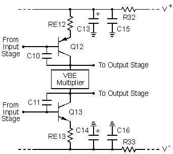
| Figure 1. Circuit diagram of the second stage. |
The diagram of the second stage is shown in Figure 1. Q12 and Q13 are complementary common-emitter stages which provide a high voltage gain to amplify the output voltages of the diff amps. Two transistors, which are part of the protection circuit, are omitted to simplify the circuit. They are normally cut off and have no effect on the operation of the second stage. RE12 and RE13, respectively, represent R21+R23 and R22+R24 in the overall circuit. The block labeled "VBE Multiplier" is discussed below. As far as the operation of the second stage is concerned, it can be considered to be a dc battery that sets the dc voltage between the two outputs.
 |
| Figure 1. Circuit diagram of the second stage. |
The output voltages from the diff amps in the input stage are applied to the bases of Q12 and Q13. The dc components of these voltages, RE12, and RE13 set the bias currents in Q12 and Q13 at 4.2 mA. The effective transconductance of Q12 and Q13 is set by this current, RE12, and RE13 at 2.5 mA/V. The ac components of the output voltages from the diff amps are in phase. When these voltages are increasing, the current in Q12 decreases and the current in Q13 increases. This "push-pull" action forces the voltage at the outputs of the second stage to decrease. Similarly, decreasing output voltages from the diff amps causes the second stage outputs to increase. Because the effective collector load impedance on Q12 and Q13 is very high, the voltage gain of the second stage is very high. It is difficult to predict a value for the gain because it is so dependent on the collector-emitter resistance of Q12 and Q13 and the current gains of the transistors in the following driver and output stages.
C10 and C11 are compensation capacitors which set the frequency of the dominant pole in the amplifier. Sometimes these capacitors are called lag capacitors or Miller capacitors. The effective value of each capacitor is increased by the collector-base capacitance of Q12 and Q13. The total capacitance of each, in combination with R7 through R10 and the diff amp bias currents, sets the gain-bandwidth product of the amplifier at about 8.5 MHz and the slew rate at 60 V/usec.
C10 and C11 are the only compensation capacitors in the circuit. Without them, the amplifier would probably oscillate. The capacitors connect between the base and collector of Q12 and Q13 where they are in parallel with the base to collector depletion capacitance of the transistors. This is the optimum place for compensation capacitors in a feedback amplifier because they have a "pole splitting" action which forces the second pole in the stage to a higher frequency. The required value of the capacitors is very small because their effective value is increased by what is called the Miller effect.
I have been asked why I did not use cascode stages (common emitter followed by common base) for the second stage. The cascode stage minimizes the Miller effect and exhibits a lower input capacitance than the common emitter stage. It is used in applications where bandwidth is to be optimized. A feedback amplifier, however, must have a dominant pole to set its gain bandwidth product. It can be shown that the optimum method to set this pole is to place a capacitor from output to input of the highest gain inverting stage. If I had used cascode amplifiers in the second stage, a capacitor would have to be placed from the output to the input of each to set the dominant pole. Then the cascode stage would have the same bandwidth as the common emitter stage. A cascode stage cannot be used to improve the bandwidth of a feedback amplifier if the gain bandwidth product is to be held constant. If the gain bandwidth product is not intentionally limited to some reasonable value, the amplifier would not be stable. That is, it would oscillate. My Double Barrelled Amplifier page shows a cascode second stage with the Miller compensation capacitors that limit its bandwidth.
R32, R33, and C13 through C16 are low-pass filter decoupling networks on the power supply rails. These filter the rail voltages to reduce the ripple voltage that reaches the input stage and second stage. The -3 dB cutoff frequency of each filter is approximately 20 Hz.
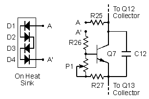
The collector bias currents in Q12 and Q13 flow through the VBE multiplier circuit shown in Figure 2. Q7 is connected as a dc voltage regulator employing shunt-series negative feedback. The dc voltage across Q7 is adjusted with P1 to set the bias currents in the output stage. D1 through D4 are mounted in holes in the heat sink with the output transistors to provide negative thermal feedback to the VBE multiplier. The diodes cause the voltage across Q7 to decrease as the heat sink temperature increases to prevent thermal runaway in the output transistors. C12 improves the voltage regulation across Q7 at high frequencies. In addition, it prevents any oscillations that might occur because of the shunt-series feedback around Q7.
 |
| Figure 2. VBE multiplier circuit. |
Many amplifiers have the VBE multiplier transistor on the heat sink with the output transistors. This eliminates the need for the diodes. The wires which run from the circuit board to the transistor exhibit capacitance to ground which can affect the high-frequency response of the second stage. At worst, this could cause oscillation problems. With the diodes on the heat sink, resistors on the circuit board can be used in series with the wires to isolate this capacitance from the second stage. These resistors are R25 and R26 in Figure 2. If Q7 were mounted on the heat sink, isolation resistors could not be used because they would affect the voltage regulation between the collectors of Q8 and Q9.
This page is not a publication of the Georgia Institute of Technology and the Georgia Institute of Technology has not edited or examined the content. The author of this page is solely responsible for the content. Copyright 2004. All rights reserved.