 |
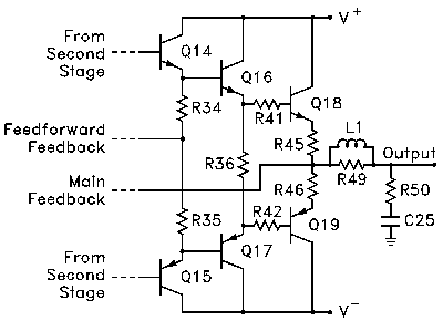
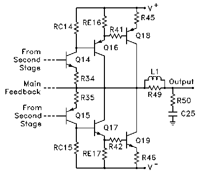
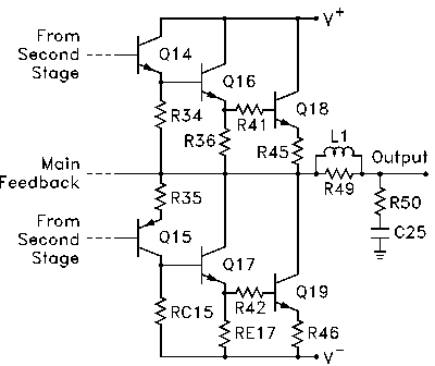
| Figure 1. Output stage. Q20, Q21, and the protection circuit are omitted. |
The two outputs from the second stage are applied to the output stage shown in Figure 1. The circuit is a three-stage complementary Darlington connection or common-collector amplifier. For simplicity, two of the output transistors (Q20 and Q21) and the elements of the protection circuit are not shown. The topology is similar to the classic JBL "T-Circuit" published by Bart Locanthi in the 1960s. I have used SPICE to simulate almost all of the topologies used for output stages, and I have found this one to be the better one. It exhibits the lowest output impedance of all of the topologies that I have looked at. This means that it can deliver more current to the loudspeaker load. And it is the least susceptable to crossover distortion.
|
| Figure 1. Output stage. Q20, Q21, and the protection circuit are omitted. |
Q18 through Q21 are the output transistors which drive the loudspeaker load. Q18 and Q20 in parallel supply positive load current, while Q19 and Q21 in parallel supply negative load current. By connecting transistors in parallel on each side of the circuit, the current rating of the output stage is doubled. The output transistors are biased in the class-AB mode. The class-A part of the mode means that all output transistors are conducting current quiescently, i.e. with no input signal. When the output voltage is driven positive, Q18 and Q20 conduct more current to supply positive load current to the loudspeaker while Q19 and Q21 progressively cut off. When the output voltage is driven negative, Q19 and Q21 conduct more current to supply negative load current while Q18 and Q20 progressively cut off. The cutting off of two transistors on alternate half cycles of the output waveform is the class-B part of the mode. When the output voltage goes through zero, all four output transistors conduct, i.e. they operate class A. This minimizes crossover distortion or center clipping on the output voltage waveform.
The three-stage complementary common-collector amplifier provides a very high current gain that is necessary to drive the loudspeaker load without loading the second stage. The voltage gain is approximately unity. Transistors Q14 - Q17 are the driver transistors which drive the bases of the output transistors. The driver transistors are connected so that they all operate in the class-A mode. This provides a low output impedance to drive the four output transistors.
The bases of the output transistors should see a low source impedance for two important reasons. First, it is necessary to supply the base currents to the output transistors that are turned on. Second, it is necessary to rapidly deplete the charge stored in the bases of the output transistors that are turned off. This forces the output transistors to turn on and off "smoothly," thus minimizing crossover distortion glitches. The bias currents in Q14 and Q15 are set at approximately 4 mA by the voltage across the VBE multiplier in conjunction with R34 and R35. The bias currents in Q16 and Q17 are set at approximately 4.5 mA by the voltage across the VBE multiplier and R36.
In some amplifiers, the transistors in the driver stage operate class AB so that they turn on and off with the transistors in the output stage. In such amplifiers, R36 would be replaced with two series resistors. The junction between these and the junction between R34 and R35 would connect to the junction between R45 and R46. This leads to an increase in crossover distortion and can cause problems with parasitic oscillations. The class-A driver stage does not have these problems.
The bias currents in the output transistors are set by the voltage across the VBE multiplier in conjunction with R45 - R48. With potentiometer P1 adjusted so that each channel quiescently draws 100 mA, the bias current in each output transistor is in the 40 to 45 mA range. This is enough current to cause all crossover distortion on the output voltage waveform with an 8 ohm load to essentially disappear. This was determined by using an oscilloscope to observe the output waveform from a distortion analyzer connected to the amplifier.
R41 through R44 are in series with the bases of the output transistors to suppress parasitic oscillations that could occur in the output stage. These are bursts of oscillations on peaks of the audio signal. Because I never had these problems with the Low TIM amplifier, my original circuit did not have these resistors. However, I did have parasitic oscillation problems with the Double Barrelled Amplifier. I found that adding 10 ohm resistors in series with the base of each output transistor solved the problem. At that time, I added them to the Low TIM circuit to be on the safe side.
R45 through R48 are emitter ballast resistors which ensure equal current sharing in the paralleled output transistors. These resistors also act as current sense resistors for the protection circuit which is not shown in Figure 1. R49, L1, R50, and C25 suppress parasitic oscillations that could be induced by shunt capacitance in the loudspeaker load. R50 and C25 mount on the loudspeaker output binding posts. On the first amplifier I built, I had these on the circuit board where they caused violent oscillations because the current through R50 and C25 generated positive feedback when it flowed through the circuit board signal ground lead. When the oscillations occurred, the heat sinks would get very hot. Moving R50 and C25 to the loudspeaker output binding posts solved this problem.
I have seen amplifier circuit diagrams with different variations of the circuit formed by R49, L1, R50, and C25. Some have R50 and C25 on the circuit side of R49 and L1. Some have a series resistor and capacitor to ground on both sides of R49 and L1. One amplifier I saw had a big inductor for L1 that was wound on a toroidal core and there was no resistor in series with C25. In the Low TIM amplifier, L1 is a very small inductor. It measures about 1 uH and looks like a short circuit for audio frequencies.
Figure 2 shows SPICE simulations of the plots of the output voltage versus the input voltage to the driver stage with and without bias voltage across the VBE multiplier. The load resistance for the simulations is 8 ohms. Without bias there is a deadband region of approximately 2.8 V in which the output voltage does not change with input voltage. This is caused by all transistors in the driver and output stages being off. With the VBE multiplier set for a quiescent bias current of about 40 to 45 mA in each output transistor, the deadband region disappears. With the bias, the slope of the curve is approximately 0.97. This corresponds to the gain of the driver and output stage. With a lower load impedance, this gain is slightly lower.
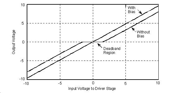 |
| Figure 2. Output voltage versus input voltage to the driver stage. |
Figure 3 shows SPICE simulations of the emitter currents in Q14, Q16, Q18, and Q20 as a function of the output voltage with an 8 ohm load. The figure illustrates how the NPN driver and pre-driver transistors operate class-A. The currents in these transistors never go to zero when the output voltage goes negative. Similar plots would be obtained for the PNP driver and pre-driver transistors.
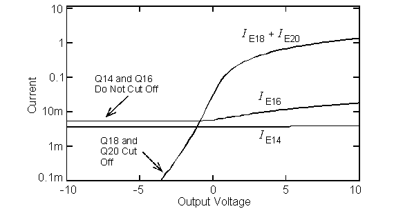 |
| Figure 3. NPN driver and output transistor currents versus output voltage. |
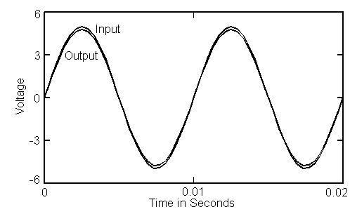
Figure 4 shows SPICE simulations of the sine wave response of the combined driver and output stages without bias current. The trace labeled Input is the input voltage, which is a 5 V peak sine wave with a frequency of 100 Hz. The trace labeled Output is the output voltage across an 8 ohm load. Without bias, the output waveform exhibits crossover distortion.
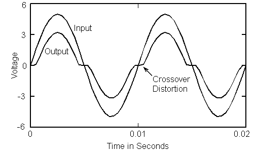 |
| Figure 4. Output voltage showing crossover distortion. |
Figure 5 shows the same waveforms with the VBE multiplier set for a quiescent bias current of about 40 to 45 mA in each output transistor. The crossover distortion is not present. The amplitude of the output waveform is less than that of the input waveform because the gain of the circuit is 0.97.
 |
| Figure 5. Output waveform with bias. |
Some of the things that have been written about class AB output stages is deceptive and downright wrong. For example, some say that the transconductance of the output stage doubles when the output signal goes through zero because all of the output transistors are conducting, and this leads to an increase in distortion. This misconception has led to the misleading term "transconductance doubling." In reality, the transconductance is not a static parameter, it varies with the transistor current. The transconductance of the output stage is defined as the slope of the plot of output current versus input voltage. The curves in Figure 2 represent plots of output voltage versus input voltage to the output stage. Because the output current is the output voltage divided by the load resistance, the slope of the curves represents the transconductance of the output stage multiplied by the load resistance. For the curve in Figure 2 labeled "Without Bias," the slope of the curve is zero in the crossover region because all transistors in the output stage are cut off. Thus the transconductance is zero in the crossover region. For the curve labeled "With Bias," the slope is constant, i.e. the curve is a straight line, thus the transconductance is constant. A properly biased class AB output stage exhibits an almost constant transconductance. You can read more about transconductance doubling by clicking here.
Builders have asked me about increasing the amplifier bias current. I don't see any problems with this. However, I do not recommend any attempt to bias it class A. If it were biased class A for an 8 ohm load, the amplifier would quiescently dissipate a little over 600 W of heat from the heat sinks for the two channels. For a 4 ohm load, the bias current would have to be doubled so that two channels would quiescently dissipate a little over 1200 W. Not only is the amplifier power supply not designed to supply this power, but also the heat sinks are not large enough to dissipate the heat. If you want to know the effect on your electric bill, get an electric heater and run it the same number of hours a day that you run your amplifier. You will be paying double if you are running an air conditioner.
Some builders have told me that they wanted to increase the bias current because they didn't feel that the heat sinks felt warm enough to the touch. If you wish to increase the bias current, follow the biasing instructions to first increase it from the specified value of 100 mA to 150 mA. Use it for a while at low power levels, keeping tabs on the temperature of the heat sinks by feeling them occasionally. If you are using a cooling fan on the heat sinks, turn it off. If you want the heat sinks to feel warmer, increase the current to 200 mA and repeat the experiment. You do not want the heat sinks to feel hot to the touch when the amplifier is used at low power levels. When feeling the heat sinks, do not touch the output transistors. You can get shocked, especially if you simultaneously touch a NPN and a PNP transistor. They have about 116 V dc across them.
I have been asked why I did not use MOSFETs in the output stage. The main reason is that the original amplifier was designed with BJTs. Because a lot of great things things have been said about MOSFETs, I did acquire a set of them which I intended to develop an output stage with. I was disappointed to find these devices plagued with parasitic oscillation problems. The manufacturers recommend putting resistors in series with the gates and ferrite beads around the gate leads to suppress these oscillations. I found these methods to be only partially effective. Therefore, I temporarily abandoned the MOSFET output stage. At this time, I tend to agree with a former student who had a great deal of experience in listening to amplifiers. He told me that BJTs sound better. He also told me that car amplifiers which are advertised as "MOSFET amplifiers" use BJTs in the output stage and MOSFETs in the switching power supply. This may not apply to all car amplifiers.
Some correspondents have asked me why I did not use an ouput stage in which the output transistors are operated in the common emitter mode. Such a stage is shown in Figure 6 where the collector of output transistors Q18 and Q19 drive the loudspeaker load. Sometimes this circuit is referred to as a complementary Sziklai connection. Transistors Q14 through Q17 are the driver transistors. Each side of the output stage consists of a common emitter stage (Q14 and Q15) driving a common collector stage (Q16 and Q17) driving a common emitter stage (Q18 and Q19). I have seen some versions of this stage in which Q16 and Q17 are omitted. These transistors provide current gain to drive the bases of the output transistors. Without them, Q14 and Q15 would have to be biased at a high current which would cause them to run hot.
 |
| Figure 6. Common-Emitter Output stage. |
If the junction between R34 and R35 is not connected to the output lead, the stage would have a high voltage gain, a very low bandwidth, and a very high output impedance. The overall amplifier would oscillate unless the gain of the output stage is reduced. To reduce the gain of the stage, widen its bandwidth, and decrease its output impedance, the junction between R34 and R35 must connect to the output lead. This adds negative feedback to each half of the stage to force it to operate at unity gain. In effect, pre-drivers Q14 and Q15 act as emitter followers to set the output voltage while output transistors Q18 and Q19 supply the load current. Some load current is also supplied by the driver transistors.
The connection of R34 and R35 to the output lead can cause the driver transistors to operate class-AB rather than class-A, which adds to crossover distortion. To see how this occurs, suppose the output voltage is going positive. The current in Q14 is increasing, which causes its base-emitter voltage and the voltage across R34 to increase. Because the VBE multiplier holds the voltage between the bases of Q14 and Q15 constant, the emitter-base voltage of Q15 decreases, causing it to cut off. This cuts off Q17 and Q19. Therefore, the lower three transistors in the output stage cut off. When the output voltage goes negative, the upper three transistors cut off. In the common collector stage of Figure 1, only the output transistors operate class-AB. The four driver transistors all operate class-A.
Because there is a local negative feedback loop around each half of the common emitter output stage, it is susceptible to parasitic oscillation problems which can occur at high frequencies where phase shifts in the two feedback loops can cause the loop gains to become positive. In effect, these phase shifts occur because there is a delay between the time that Q14 and Q15 set the output voltage and the time that Q18 and Q19 supply the output current. This delay is caused by the internal capacitances of Q18 and Q19. Because Q18 and Q19 are connected in the common-emitter mode, the Miller effect causes the internal capacitances to be much larger, thus slowing down the response of the output transistors and increasing the delay in their collector output currents. Because the output transistors have the largest internal capacitances and the lowest gain bandwidth product, it only makes sense to me to operate them in the configuration that they exhibit the widest possible bandwidth. That configuration is the unity gain common collector connection.
Back in the days when audio kits were popular, there was a line of amplifiers called Tiger Amps sold by a company named Southwest Technical Products Corporation (SWTPC). Some of these amps used common-emitter output stages which had local feedback around the output stage to cause it to operate at a voltage gain of 4. This was achieved by adding resistors from the emitters of Q14 and Q15 to ground so that only a fraction of the output voltage is fed back to the emitters. These amplifiers were very unstable, causing them to oscillate, overheat, and blow tweeters. Walter Jung tested one of the SWTPC Tigersaurus Amps for the Audio Amateur. His concluding comment in his review was, "Dan Meyer, where are you?" Dan Meyer was the founder of SWTPC. His original company name was Demco, but the General Motors Delco Radio Division brought a lawsuit against him to force him to change the company name. The company went out of business after getting into the home computer market.
A hybrid output stage that uses a common-collector stage for positive output current and a common-emitter stage for negative output current is shown in Figure 7. This stage is called a quasi-complementary output stage. The pre-driver transistors are Q14 and Q15, which are npn and pnp complements. The driver transistors are Q16 and Q17. The output transistors are Q18 and Q19. These are all npn types. This stage was commonly used in early amplifiers when rugged high current pnp output transistors were not available. The Crown DC-300 amplifier series is a good example. The stage is still used in some amplifiers today. Some versions that I have seen omit Q16 and Q17. Without the current gain provided by these transistors, Q14 and Q15 would have to be biased at a high bias current, which would cause them run hot.
 |
| Figure 7. Quasi-complementary output stage. |
I have seen one "high end" amplifier in which the transistors in the driver stage ran so hot that the circuit board was charred around the transistor solder joints. If I can't hold my finger continuously on a transistor on the circuit board, it is too hot. Hot transistors are a recipe for premature failure. The "high end" amplifier had self destructed several times. The last time I saw it, it had taken out an expensive set of new loudspeaker drivers.
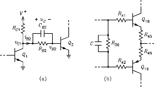
Some people have asked me if the addition of a capacitor in parallel with R36 will improve the switching time of the transistors in the class-AB output stage. Speedup capacitors have been commonly used with transistor switches to improve the cutoff time of the switch. Fig. 18(a) illustrates such a switch. Transistor Q2 is the switch. Its collector load is not shown. When Q1 is cut off, iB2 flows and cuts transistor Q2 on. The flow of iB2 causes the capacitor to charge to a positive voltage, i.e. vC > 0. When Q1 saturates, vC1 = 0 which makes vB2 = -vC. The negative voltage at the base of Q2 sucks out the charged stored in the base region of Q2, which causes it to cut off faster. When Q1 is off, the voltage to which CB2 charges is determined by the ratio of RB2 to RC1. If the emitter of Q2 were connected to a negative voltage source, then RB2 and CB2 could be omitted because vB2 would be forced to go negative when Q1 saturates. Therefore, speedup capacitors are needed only when a single polarity power supply is used with transistor switches.
 |
| Figure 8. (a) Transistor switch. (b) Simplified output stage. |
Fig. 8(b) shows a simplified diagram of the amplifier output stage (the driver transistors are omitted) with a capacitor shown in parallel with R36. Because the VBE multiplier holds the voltage across R36 constant, the addition of the capacitor has no effect on the voltages at the bases of Q18 and Q19. If speedup caps are necessary, they should be added in parallel with R41 and R42. However, these 10 ohm resistors are too small for the speedup caps to have any effect. In addition, the caps would defeat the purpose of R41 and R42, which is to suppress parasitic oscillations. A capacitor in parallel with R36 will not speed up the switching speed of the output stage. Speedup capacitors are not needed in circuits which have bipolar power supplies because voltages of both polarity are available to drive the transistor bases.
This page is not a publication of the Georgia Institute of Technology and the Georgia Institute of Technology has not edited or examined the content. The author of this page is solely responsible for the content.